Navigation

University of Rome
Tor Vergata

TIBERCAD PROJECT
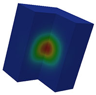
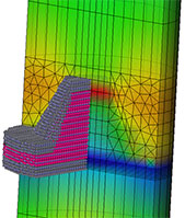
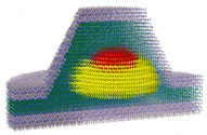
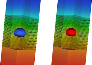
tiberCAD is a multiscale CAD tool for the simulation of modern nanoelectronic and optoelectronic devices.
tiberCAD project has been developed in the OLAB research group, in the Department of Electronic Engineering of the University of Rome "Tor Vergata", based on its long-standing experience of 20 years of device simulations and development of simulation software. Main Research topics of OLAB are the design, fabrication and characterization of active optoelectonic and nanoelectronic devices.
Until 2024 tiberlab S.r.l., a spin-off of University of Rome "Tor Vergata", has been dedicated to the commercial exploitation of this software technology. During 2024, it has been decided to make tiberCAD open source, and the software has been made freely available upon request. The sources will soon be uploaded to github.
The current version can be downloaded here: tiberCAD-3.4.0-x86_64-linux_installer.sh
On these pages you will find API documentation, SDK, tutorials and other resources.