Navigation

University of Rome
Tor Vergata

Multiscale Simulation of MOSFETs based on high-k oxides
In the following we will show an advanced application of tiberCAD which involves atomistic calculations based on the Empirical Tight Binding (ETB) approach.
This feature is not yet implemented in the current version 2.0, but it will be available from the next tiberCAD release.
Here we present a multiscale simulation approach to simulation of MOSFET devices. This kind of simulation includes both macroscopic drift-diffusion current model and quantum tunneling model. The models are solved together in a self-consistent way. As an example, we study the subthreshold transfer characteristics of MOSFETs based on high-k oxides. We compare the high-k gates based on HfO2 and ZrO2 with a SiO2 gate of the same equivalent thickness and show the effect of the gate oxide tunneling current on transistor performance.
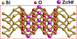
Microscopic atomic Si/ZrO2/Si and Si/HfO2/Si MOS structures have been constructed basing on the crystalline cubic forms of the oxides. The interface model applied assures that neither dangling bonds nor interface states are present, so that there are no states in the bandgap of Si.
Tunneling properties of ZrO2 and HfO2 high-k oxides are calculated by applying the empirical tight-binding (TB) method, embedded in a transfer-matrix-type scheme.
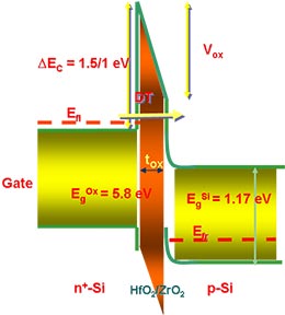
If we consider a n+-Si/high-k-oxide/p-Si MOS capacitor biased in the accumulation region, with a negative voltage applied to the gate terminal, tunneling consists of electrons flowing from the gate to the p-Si region.
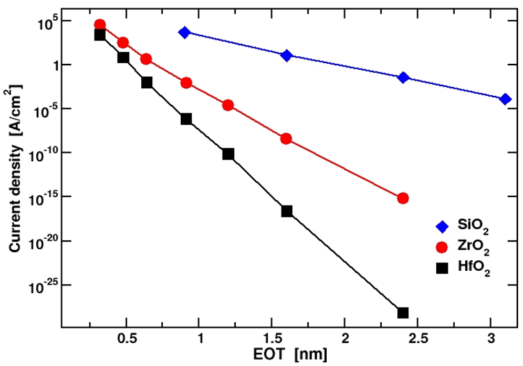
The equivalent oxide thickness (EOT) dependence of TB tunneling current is calculated for both ZrO2 and HfO2 based MOS structures. Very low gate leakage currents are found for high-k oxide MOS systems, in comparison to SiO2-based structures with an equivalent oxide thickness and the same bias.
Two different models for transport phenomena are used in the simulation of MOSFET transistor: a semi-classical one to describe electron transport in the semiconductor and a quantum-mechanical one, based on the TB atomistic model shown before, to describe transport in the nanometer-scale gate oxide. The semi-classical transport model implemented in tiberCAD is based on a drift diffusion description assuming local thermal equilibrium of electrons and holes. The nonlinear Poisson and current continuity equations are discretized on a finite element grid and solved using a Newton type algorithm.
The semi-classical and quantum-mechanical models are coupled in the following way. First, Poisson's equation is solved on the whole device. Then the tunneling current is calculated quantum-mechanically. We assume that tunneling current density at an element boundary that separates oxide and semiconductor depends only on the barrier height and the Fermi energy at the element. This allows us to compute the tunneling current density independently for each finite element at the boundary.
The obtained current is used as a boundary condition for the next drift-diffusion calculation in the semiconductor channel. Then the tunneling current is computed again for the new values of the electric potential and the Fermi energy. This procedure is repeated until convergence is reached.
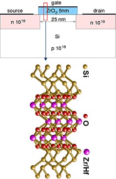
The simulated MOSFET device has a 5 nm thick ZrO2 (HfO2) gate oxide. The channel is 25 nm long and is p-doped with a concentration p=1018 cm-3.
Let's consider the tunneling influence on the subthreshold current. The subthreshold transfer characteristics, for a source-drain voltage of 0.1 V, are calculated with and without including the gate oxide tunnel current. Results for ZrO2 are compared with HfO2 and SiO2 with the same EOT.
![]()
![]()
The SiO2 gate shows significant tunneling with respect to the HfO2 gate, but the ZrO2 tunneling current is visible only at small source-drain voltage.
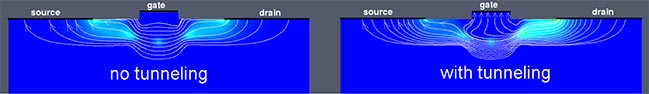
Here the current flow lines are indicated, showing the flowing of tunneling current through the gate oxide (corresponding to a tunnel flow of electrons from the gate to the Si substrate), in accumulation bias conditions.
References
- M. Auf Der Maur, M. Povolotskyi, F. Sacconi A. Pecchia and A. Di Carlo - Multiscale Simulation of MOS Systems based on High-k Oxides, Journ Comp. Electronics (2007)
- F. Sacconi, J.M. Jancu, M.Povolotskyi, A. Di Carlo - Full band tunneling in high-k oxide MOSstructures, IEEE Trans. Electron Dev., in press (2007)
- F. Sacconi, A. Di Carlo, P. Lugli, M. Stadele, J.M. Jancu - Full band approach to tunneling in MOS structures, IEEE Trans. Electron Dev., 51 (5), 741-748, (2004)